Announcement

Collapse
No announcement yet.

HV SS Regulators?

Collapse
X
 
  • Filter
  • Time
  • Show
Clear All
new posts

  • #16
    OK, just checking. It gets much smaller with SMD, but I thought I'd ask.

    Next: PCB style. I laid out both circuits on the same sized PCB, 2.8" x 1/8". The power density is the same, but of course one has just a bunch of 5W zeners, the other has a bunch of little zeners and two more MOSFETs. Here are pics of the two designs:
    Click image for larger version

Name:	MHuss Reg Sch.jpg
Views:	1
Size:	195.7 KB
ID:	857538Click image for larger version

Name:	MHuss Reg PCB.JPG
Views:	1
Size:	158.0 KB
ID:	857539
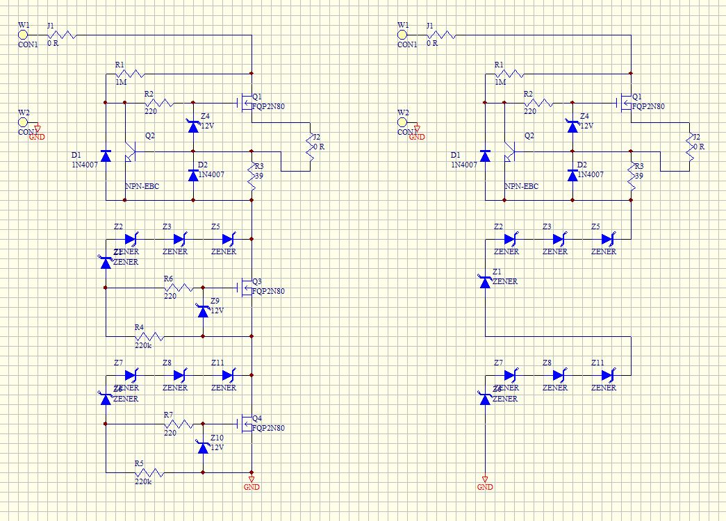
    On the schematics, note that they differ only in that the three-MOSFET version has two more MOSFETS, two gate protection zeners and four more 1/4W resistors. It is technically possible to use one circuit board for both (i.e. the 3-MOSFET version) and install jumpers to convert.
    The zener-only variant is to spread the heat from the power zeners out on the board.

    Boards are missing any kind of mounting provisions, so until I put some mounting holes or such into them, they're suitable only for velcro mounting.

    Forgot to mention: In spite of the allure to tube-amp guys of the few-zeners version, I consider it less reliable based on experience with power zeners. Zeners used at anything like their rated power and current are IMHO inherently unreliable. Adding the extra parts in the 3-MOSFET version does add other failure points, true, but it also adds a great deal of control, and that lets a designer foresee and cope with accidents.
    Amazing!! Who would ever have guessed that someone who villified the evil rich people would begin happily accepting their millions in speaking fees!

    Oh, wait! That sounds familiar, somehow.

    Comment


    • #17
      Very cool. I agree the 3 FET version is probably better, and reliability is a top concern.

      I'm getting conversant with KiCad, and have been getting good, inexpensive 2-sided PCBs made at OSH Park, so I can run with your design/layout once you consider it ready to go.

      I hate sounding like a broken record, but thanks so much for your help.

      Comment


      • #18
        Works fine. You can take that and run with it if you like, or we can just iterate a couple of times and I'll send you gerber.

        More considerations:
        I need to make you up a parts list. Some of the parts are out of the usual mainstream, but all are available through Mouser. There are some substitutions that can be made, and adjustments that can be made.

        The TO-220 will just barely not dissipate enough heat to be reliable in this app. I set the board up for one heat sink per TO-220. It's a little lie-flat device, Mouser number 984-ATS-PCB1069 ($0.44) that fits into that rectangle around the MOSFETs. It'll get the MOSFETs up to about 4-5W capability, enough for the 2-3W they will actually have in this application. The MOSFETs are Mouser 512-FQP2N80 ($1.20).

        Gate zeners ("12V") are whatever you like. I'd get the cheapest DO-41 or smaller nominal 10V-12V. Voltage is not critical as long as it's not bigger than maybe 15V.
        The other zeners in the MOSFET version can be 500mW or even lower; 1W may be OK too, and both of these are relatively cheapest sizes. Smaller than 500mW and they don't make them in high voltages. Bigger than 1W-1.3W and they cost more. All of the zeners in the MOSFET version can be found in 500mW. I have a list somewhere...
        The nice thing about funneling all the power into the MOSFETs is that the other parts get really low power. I actually looked for 100mW zeners, which would be plenty. But they don't make those in higher voltages.
        Resistors can be 1/4W or 1/8W.
        The "middle" MOSFET active zener only needs two zener diodes in the string. I put in four spaces for them to allow some flexibility in case you need to adjust voltages.
        I put in two wire jumpers on the theory that you might want to do a bathtub etch. If you're going to a commercial outfit for double sided, plated through, those could be eliminated and replaced by some top-side traces.

        There are more circuit quirks. Yell if anything doesn't make sense.
        Amazing!! Who would ever have guessed that someone who villified the evil rich people would begin happily accepting their millions in speaking fees!

        Oh, wait! That sounds familiar, somehow.

        Comment


        • #19
          Sounds good. If you can provide a BOM I'll gen up a Mouser order.

          Comment


          • #20
            Here's an updated schemo and BOM. I can send more detail on the layout if you need it.

            MHuss Regulator Schm - BOM.pdf
            Amazing!! Who would ever have guessed that someone who villified the evil rich people would begin happily accepting their millions in speaking fees!

            Oh, wait! That sounds familiar, somehow.

            Comment


            • #21
              Excellent. Thank you.

              Comment


              • #22
                Being stupid at times, I'll do all the math after the fact instead of before when I should have.

                I just did some rough calculations and it looks like the higher voltage output will draw something like 6-8mA total (four triodes total). Can a simple change be made to accommodate this? (The lower voltage will be around 3mA total).

                Comment


                • #23
                  I use that technique a lot myself.

                  The answer is yes, it's easy. The current limiter can easily be set to let through more current. R3 is 39 ohms for a total of 15ma. You can twiddle that value to change the max current. After that, the only question is whether the MOSFETs will overheat when all the triodes they're supplying are pulled out.

                  15ma is probably a bit of overkill on my part. Zeners and zener-like things hold the voltage relatively constant until the zener gets starved for current; then the voltage drops. There's a total of about 15ma being let through the string of top and bottom zeners, just so there is some current in the zeners at all times. 5ma is where I put that, so you might have your 6-8ma from the top zener as is. If not, put a resistor in parallel with the 39 ohm resistor to juice up the current a little. Paralleling with a 140 ohm resistor would increase the current up to about 19ma, for instance. But strictly speaking, the existing setup is probably good up to 5ma out of the lower zener, 8ma out of the top one.

                  The only issue keeping you from setting whatever current you want with those MOSFETs is getting the heat out of them. They are probably good for an 500ma each with a (really, really) good heat sink on them. They're heat

                  The total power going into the zener sections with a limit at 15ma is 15ma times 390V, or 5.85W. If there is no current going out of the zener outputs, the zener MOSFETs have to eat all that power and dissipate it into the air through the heat sinks. This can happen when all the triodes are pulled out. So the dissipation on the zeners is the current limit times the voltages. The top zener dissipates 1/3 of the power (because it has 1/3 of the voltage) and the bottom one 2/3.
                  If we say that the total power is 6W, the top zener is two watts and the bottom one is 4W. The shorter heat sink (ATS1069) is probably fine at up to 4 W and the taller one (ATS1070) would give some thermal reserve. A lot depends on how they're mounted in the box. Best is if the PCB is mounted vertically so air can chimney up from the heat.

                  Bottom line, the taller heat sink gets you there even if you have to up the current limit a few ma.
                  Amazing!! Who would ever have guessed that someone who villified the evil rich people would begin happily accepting their millions in speaking fees!

                  Oh, wait! That sounds familiar, somehow.

                  Comment


                  • #24
                    Good to know, thanks. I did order the taller heat sinks, because any SSD can never be too un-warm.

                    Comment


                    • #25
                      Dead right, that.
                      Amazing!! Who would ever have guessed that someone who villified the evil rich people would begin happily accepting their millions in speaking fees!

                      Oh, wait! That sounds familiar, somehow.

                      Comment


                      • #26
                        Aaack, the back of the FETs are connected to the source terminal. Should I leave the heat sinks 'live,' or put in insulators? I think I have some TO-220 ceramic ones.

                        Comment


                        • #27
                          Sorry - I didn't check back in for a couple of days.

                          I think it's the drains that are connected to the back/tab of the MOSFETs, but that is effectively the same problem. If I were building this, I would just leave the sinks live, with only a little heat sink goo between the device and the sink. This is going inside the chassis of a tube amp, and there are lots of other points in there that are live with DC high voltages. I did the proposed layout assuming that the sinks would be live.
                          Amazing!! Who would ever have guessed that someone who villified the evil rich people would begin happily accepting their millions in speaking fees!

                          Oh, wait! That sounds familiar, somehow.

                          Comment


                          • #28
                            Agreed. I'll just have to make sure it's well mounted!

                            Comment


                            • #29
                              So, I got the boards back and populated one. Hooked it up to 500v, output voltages measure correct.

                              Put it in the amp, connect it all up, turn it on, voltages still look good.

                              Put a sine wave in and there's some hash on the amp output. After probing a bit I found out this noise is present on both voltage outputs.

                              Picture attached, 20mV/div (x10) and .1ms/div.

                              Any ideas? FWIW, The only component I subbed is I used an MPS A06 instead of the 2N3904, which has equal or greater ratings.
                              Attached Files

                              Comment


                              • #30
                                I've been resisting the urge to ask how it's going with these.

                                I can speculate that maybe this is the inherent zener noise being buffered by the MOSFETs. My first step would be to put a cap across the zeners and see if any of the noise changes. I'd try the biggest film cap you have that will handle the voltage.

                                Reflecting a bit, it may be that I got the zeners at such a low current inside the zeners that they're in a noisy region of their operation.
                                Amazing!! Who would ever have guessed that someone who villified the evil rich people would begin happily accepting their millions in speaking fees!

                                Oh, wait! That sounds familiar, somehow.

                                Comment

                                Working...
                                X