Ad Widget

Collapse

Announcement

Collapse
No announcement yet.

Furman parametric eq distorted

Collapse
X
 
  • Filter
  • Time
  • Show
Clear All
new posts

  • Furman parametric eq distorted

    Hi all:
    I have a Furman PQ6, stereo version of the PQ3 and can find no schematic anywhere. So I am attempting repair without.
    The problem is the output is heavily distorted. Even with the eq switched out, the signal is still the same using a signal generator and scope.
    There are 9ea LM353 op amps on each of the 2 boards which are identical.
    I follow the input to the board and almost immediately the sine wave becomes unrecognizable.
    From the point of entry on the board, the trace goes to a 2.2K resistor, and on the other side of the resistor goes to 2 different diodes.
    The waveform is ok on the primary side of the resistor, and sharply distorted on the other where the diodes are.
    If I lift one end of the diodes, the waveform becomes normal on the secondary side of the resistor.
    This circuit goes to the 1st op amp on pin 2. The op amps are socketed and removing them has no effect except to interrupt the output.
    My question is: I should see a nice sine wave at different levels throughout the circuit, correct?
    And especially that early on in the circuit?

  • #2
    Now we have a schematic, thanx Jazz P Bass! Deleted guesses, all incorrect. On Furman's low level input, there's a pair of back to back diodes across the inputs to a gain stage op amp. These act as a rough limiter, aka "fuzz box", so the signal can be no larger than the breakover voltage of those diodes, 0.6 volt for silicon. Mind, that's 0.6V peak-to-peak not average. So, if you're inputting a signal that exceeds this level, the diodes will square it off and that's to be expected. Try a small test signal, read the output of op amp A101a, you may find everything's A-OK. There's always the possibility the op amp's faulty, but with this knowledge in mind you can test your Furman's low level input properly.

    PQ6 is one of the first commonly available parametric EQ's, an invaluable piece of production gear, now a bit of a collectors' item. Hope you can get it running right.
    Last edited by Leo_Gnardo; 02-08-2017, 02:36 PM.
    This isn't the future I signed up for.

    Comment


    • #3
      Since we have no schematic, where do the diodes go? Does the other side go to ground? Are they maybe clamping diodes? Have you tested them and are they good? If you remove them and the waveform becomes "normal", it sounds to me like you might have leaky or shorted diodes.
      "I took a photo of my ohm meter... It didn't help." Enzo 8/20/22

      Comment


      • #4
        I'll believe the diodes are clamps to +15 and -15, easy enough to check with a meter. ANd no need to replace them yet, just measure that resistor from the input. It either has 15v on it or not. Hopefuly not. Find 15v there, one of the diodes is shorted.

        Meanwhile have we bothered yet to check the +15 and -15v supplies AT THE CHIPS for voltage level and ripple?
        Education is what you're left with after you have forgotten what you have learned.

        Comment


        • #5
          Here is the PQ3_6 schematic.

          The complete manual can be found here: https://www.google.com/url?sa=t&rct=...46496531,d.eWE
          Attached Files

          Comment


          • #6
            As you said this is a stereo unit, are you looking for a fault on one side or both sides?
            If it's just one side, then you can compare to the good side, no need for any speculation about what is normal.
            Originally posted by Enzo
            I have a sign in my shop that says, "Never think up reasons not to check something."


            Comment


            • #7
              If both sides are distorting, try turning the Gain way down.

              Comment


              • #8
                Just checked the schematic (thanks JPB ) Diodes D101/102 are across A101a Op Amp inputs so they will not clip even with input signal 600mV peak , as long as said Op Amp works properly and/or input signal exceeds Op Amp common mode range (think some 12/13V peak) .
                That said, one or both might be shorted or said Op Amp might be bad (or NFB open).
                In any case, apply 100mV RMS to low level input and follow them.
                Juan Manuel Fahey

                Comment


                • #9
                  Thanks for the link and schematic. Very helpful!

                  Comment


                  • #10
                    I replaced the diodes but was putting too hot a signal into the unit. Now it seems all is well, Thanks to each of you

                    Comment


                    • #11
                      This unit started acting up again. Unfortunately the schematic listed above is not the same as my unit, not at all. Perhaps this is a earlier design? Anyway the right channel when engaged has a much lower output than the left. Turning it up only causes it to distort, but no increase in output. This is using the low level input with a low signal, or the high level input with a larger input gain.
                      I have compared the two channels with a o-scope but difficult to see much difference, and then only at the places close to the output terminals. Without a schematic its very difficult to see where the change is occurring. I have tried swapping some of the op amps between boards to no avail.
                      I have also checked nearly every component on both boards with an ohmmeter. Found no significant differences in the values.
                      When I turn off (bypass the eq and it's pre amp) the output signal increases
                      Stumped!

                      Comment


                      • #12
                        Unfortunately the schematic listed above is not the same as my unit, not at all.
                        Really?
                        Basic circuit should be very similar, not too many ways to make a parametric equalizer and circuit shown is basically the textbook/datasheet example; plus a preamp at the input to accept low or high level signals and a mixer + attenuator at the output for the same reason.

                        Maybe parts designation is different, dunno (as in the first Op Amp being called IC1a insted of A101a or whatever), that does no change the real circuit.

                        In principle, follow tracks from low level input jack, where do they lead to?
                        They "should" go to an Op Amp input. How is it labelled on PCB?
                        Please post a closeup picture of it and surrounding parts.
                        If board is Epoxy Glass itīs greenish translucid, a well placed lamp may show tracks and parts.

                        Inject 100mV 1kHz
                        Does signal reach Op Amp input clean? (pins 3 or 6)

                        You should find clean signal, some 10X stronger , on associated output pins 1 or 7 respectively.
                        And so on .
                        Also check hot pin of input level potentiometer, output of the Op Amp right after it (follow the tracks), at each band gain stage output (they are the ones feeding the frequency pots), they would be A103/105/108 pin 1 , also main output mixe pins 1 and 7

                        As you see, I couldnt care less about schematic or PCB designations, just where they are and what are they connected to.

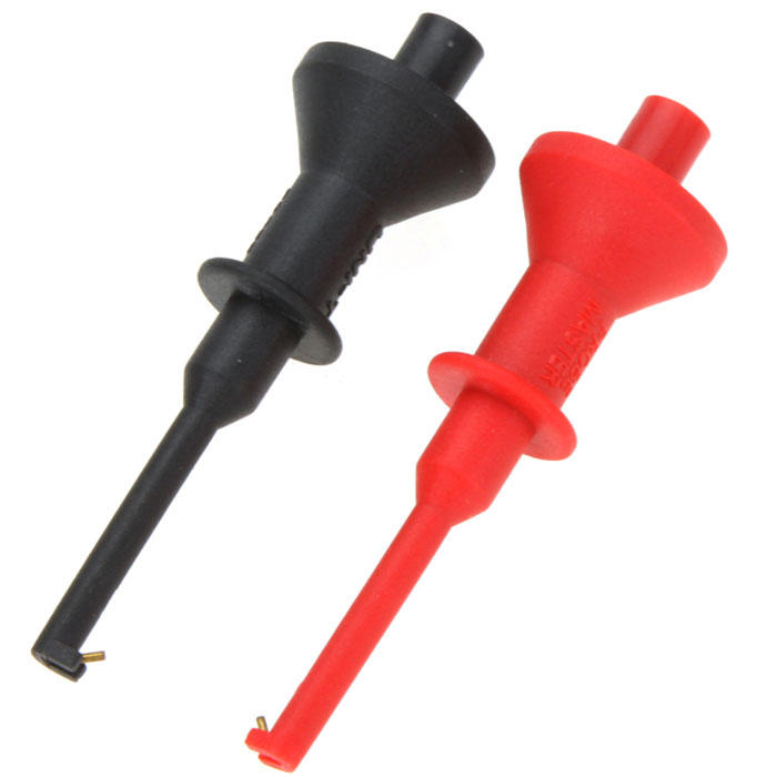
                        I guess those ara all through hole parts, so this kind of probe should help you:


                        You may even use fine point Sharpie to follow the audio tracks , comparing PCB and schematic, and worst case if they differ, tracing and trusting PCB audio path.
                        Juan Manuel Fahey

                        Comment


                        • #13
                          Maybe parts designation is different, dunno (as in the first Op Amp being called IC1a insted of A101a or whatever), that does no change the real circuit.

                          The 9 ea LF353N op amps are labeled A,B,C,,,,I.

                          In principle, follow tracks from low level input jack, where do they lead to?
                          They "should" go to an Op Amp input. How is it labelled on PCB?
                          Please post a closeup picture of it and surrounding parts.
                          If board is Epoxy Glass itīs greenish translucid, a well placed lamp may show tracks and parts.


                          Point to point wiring to the board, thru a 2.2k resistor and on to pin 3 of op amp "I"


                          Inject 100mV 1kHz
                          Does signal reach Op Amp input clean? (pins 3 or 6)


                          Yes its clean on pin 3


                          You should find clean signal, some 10X stronger , on associated output pins 1 or 7 respectively.
                          And so on .


                          Yes, the gain is there. In fact it appears that the outputs are all there in varying gain levels depending on frequency.

                          Also check hot pin of input level potentiometer, output of the Op Amp right after it (follow the tracks), at each band gain stage output (they are the ones feeding the frequency pots), they would be A103/105/108 pin 1 , also main output mixe pins 1 and 7

                          As you see, I couldnt care less about schematic or PCB designations, just where they are and what are they connected to.


                          You may even use fine point Sharpie to follow the audio tracks , comparing PCB and schematic, and worst case if they differ, tracing and trusting PCB audio path.[/QUOTE]

                          The only place I can find an obvious difference in signal between the 2 boards is just before the high gain output, labeled "30".
                          Following it back to pin 1 on op amp labeled "H".
                          Signal from there to high gain output jack and surrounding circuitry is all attenuated compared to the left channel.
                          Pin 3 just looks like hash. And I have swapped op amp "H" between the channels with no change.
                          Click image for larger version

Name:	IMG_20190302_182003[1].jpg
Views:	1
Size:	3.38 MB
ID:	853225
                          In the pic green is the output jack circuit back to pin 2 on op amp "H". yes pin 2
                          The pin 1 circuitry is highlighted in red
                          I will continue to double check everything you suggested, but in order to keep this brief I've jumped ahead to point the difference points out.
                          Again Hash on both boards, op amp "H" pin 3. Pin 1 on same is attenuated greatly on left channel. All knobs set same.
                          Perhaps this is a trimpot issue?

                          Comment


                          • #14
                            Good, thatīs the sloooowww but sure way to solve it, in absence of a proper schematic.

                            Those are very old fashioned PCBs "drawn" by sticking (yes, with your fingertips) narrow ribbons made out of black crepe paper (think very narrow painterīs paper tape) on a transparent acetate sheet.
                            All the rage in late 70's early 80īs PCB design, most famous ones made by Bishop Graphics.
                            All before widespread home PCs .

                            lacking a schematic, youīll have to continue following signal, step by step, forwards or backwards your choice, until you find *one* stage where it changes from good to distorted.

                            As Enzo often says, maybe you donīt even have a bad *part* but a bad *connection* ,or a "mechanical" part such as a pot/jack/switch/connector.

                            Try to avoid or keep to a minimum pulling/replacing parts at random unless quite certain you are in the proper defect area, those very narrow tracks and small pard are EASY to tear away or simply crack.

                            But you are going the right way, it will take patience though.

                            Post some component side pictures, showing the tracks by transparency, a couple white Leds at the end of some cable can help a lot if space is tight. Or a piece of Led strip.

                            And I bet if you print a large (maybe 2 sheets taped together) schematic copy, you will be able to write on it actual part valuyes and designations.

                            I bet the 2k2 input resistor you mention is R101 ; the "A" Op amp receiving signal on pin 3 is A101a and so on.

                            You may relabel all parts on the "official" schematic and scan it for us (and your own use).

                            Some parts may be not present, I see empty holes in the PCB, but basic circuit should not differ much,if at all.
                            Juan Manuel Fahey

                            Comment


                            • #15
                              Your first attachment in post #13 is not working
                              (right under where you said 'Point to point wiring to the board, thru a 2.2k resistor and on to pin 3 of op amp "I" ')
                              Originally posted by Enzo
                              I have a sign in my shop that says, "Never think up reasons not to check something."


                              Comment

                              Working...
                              X